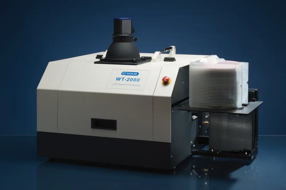
Lifetime Tester (WT) systems are advanced and versatile measurement platforms designed to perform a wide range of material characterization tasks, including carrier lifetime measurement, resistivity mapping, metal contamination detection, and other critical semiconductor property evaluations. These systems combine multiple measurement techniques and come with all accessories necessary for mapping, to deliver comprehensive wafer analysis for both research and industrial applications.

Each system can be configured based on the user’s requirements by adding measurement capabilities and automation capabilities described below. Get in touch and find your perfect WT-2000 configuration!

  • Carrier Lifetime Measurement (eg.PCD techniques): Determining the effective minority carrier lifetime, a key indicator of material quality and defect density, crucial for both silicon and compound semiconductor substrates, eg. SiC.
  • Contamination Monitoring with Surface PhotoVoltage technique (SPV)
  • Resistivity Mapping: Non-contact (eg. Eddy) and contact (4pp) methods to map resistivity variations across the wafer surface.
    Sheet Resistance Measurement (eg. JPV): Essential for assessing electrical uniformity and doping profiles on semiconductor wafers and solar cells.
  • Quality Control: Robust and precise monitoring of wafer and solar cell quality throughout production lines.

  • Multi-Method Capability:Enables use of various measurement principles within one system to suitdifferent material types and characterization needs.
  •  Contamination monitoring withmultiple different measurement methods, eg. µ-PCD, c-PCD, and offeringdifferent wavelength laser options tailored for different materials.
  • Crystal defect detection
  • Key feature of SPV is bulk Fedetection, and charge carrier diffusion length measurement
  •   Implant process monitoring withJPV sheet resistance measurement
  •  Electrical characterizationwith contact (4pp) and non-contact (Eddy) methods for bulk and thin film applications
  • Automation software withSECS/GEM communication option
  •  High Sensitivity &Accuracy: Critical for identifying defects and contamination affecting carrier lifetime and device performance.
  • Flexible Application: Suitablefor research and production environments, supporting wafers from laboratory samples to industrial-scale manufacturing.
  • Comprehensive Data Analysis:Integrated software for mapping with all offered metrologies, analysis, andreporting facilitates rapid process optimization and quality control.
  • Wafer size: up to 300 mm 
  • High-resolution mapping
  • Automation options: manual oroptional automation
  • Wafer loading is possible from 13 or 25 slot cassette including FOUP, FOSB, and open cassettes for 100-300 mm wafers
  • Each system can beconfigured based on the user’s requirements by adding measurementcapabilities and automation capabilities described below. Get in touch fordetailed technical specifications.
  • Semilab offers WT optionsdesigned for specific applications:
    •  WT-2000PVN for photovoltaic applications
    • WT-2000MCT for temperature dependent lifetime measurement for characterization of narrow-band semiconductors
    • WT-2010D with all the metrology of WT-2000 designed for crystalline silicon blocks, size up to 210x210x500 mm

No items found.

Contact us for Information and Pricing

Get expert advice and tailored solutions for your research needs