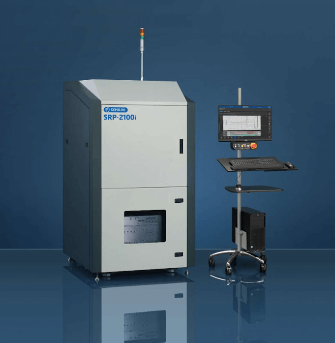
SRP-2100 / SRP-2100i Spreading Resistance Profiling

iPhone mockup

The SRP-2100 series is Semilab’s flagship solution for high-precision spreading resistance profiling (SRP) and dopant concentration analysis in semiconductor wafers. Suitable forsilicon and compound semiconductors (with PCIV option), it delivers fully automated, accurate depth profiling for process monitoring, failure analysis,and device characterization.

  • Process control: Advanced process monitoring and tuning in semiconductor fabs
  • Failure analysis: Accurate dopant and resistivity profiling for device troubleshooting
  • Research & Development: Profiling of multilayer and compound semiconductor structures
  • Characterization: Depth profiling of junctions, transition zones, and multilayer stacks

  • Fully automated measurement cycles with manually automated probe and sample alignment
  • Operator-friendly, easy-to-use interface: Expert supervision recommended for evaluation
  • Compact Footprint with effective, high-quality vibration and acoustic isolation
  • Multipurpose: Suitable for multilayer structures, no thickness limitations
  • High resolution: Nanometer scale depth resolution, high spatial accuracy
  • In-situ Bevel Angle Measurement (BAM): Standard feature for precise junction depth analysis
  • Stand-Alone Bevel sample polishing unit
  • Options: PCIV option for wide bandgap and SOI application, which combines variable measurement bias and current-voltage curve analysis to measure spreading resistance profile on novel semiconductor materials
  • Iterative PCIV software option (iPCIV): designed to measurehighly variable samples with very high resistance value (ideal below 1E-11 Acurrent range),
  • Shallow Layer Measurement (SLM): extending the SRP techniqueto determine thin layer structure,
  • Variable Probe Spacing (VPS): motorized probe spacingmovement allows the measurement of sheet resistance of thin isolated layers
    • Temperature-controlled measurement chamber (TCM),
    • Signal Tower: standard industrial signal tower which gives information on system status

Measured parameters:

  • Dopant concentration and resistivity on Si materials
  • Carrier density and resistivity profile shape
  • Resistance profile on compound semiconductors: AlGaAs, GaAs, GaN, Ga2O3, InP, SiC
  • AlGaN/GaN HEMT structures
  • Junction depth
  • Transition width
  • Sheet resistance
  • Electrically activated dose
  • Bevel Angle Measurement (BAM)

No items found.

Contact us for Information and Pricing

Get expert advice and tailored solutions for your research needs